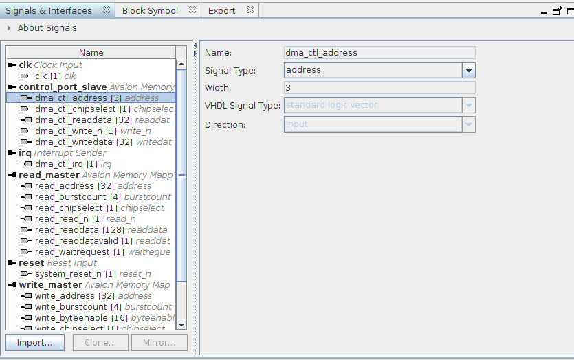
I’ve connected a DMA to manage the write and read operations between the FPGA and HPS using the FPGA-to-HPS SDRAM interface (image 1 below) found on the HPS. Does anyone know what the dma_ctl_address represents and why its only 3 bits (image 2 below) ? I’ve looked through the generated verilog ip files as well as gone through the online documentation, but found no explanation of this 3 bit addressing scheme. Does anyone know what this address refers to if I want the DMA to handle the communication with the f2sdram0 port from the FPGA ?
Also I should mention I am fairly new to Quartus, Qsys, etc and as such I may have this setup very incorrectly (the base template for this project works/tested). In this situation please let me know if I am using the DMA incorrectly.
Image 1:
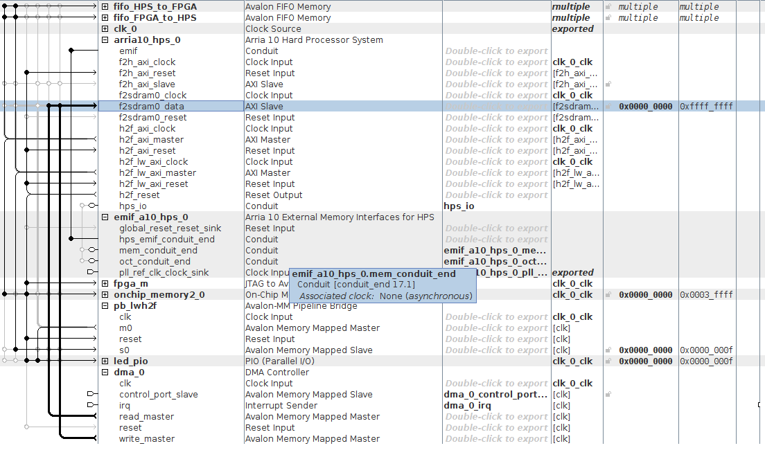
Image 2: