HPS and FPGA communication Arria 10 SoC

Hello :slight_smile: ,

I’m working on project in which i need to create a communication between HPS and FPGA, the platform i’m using is Arria 10 SoC, i’m a beginner to SoCs , i need to send information from HPS to FPGA than the FPGA will process these informations (input) and send the output back to the HPS .
so what i’m asking for is how to begin to perform this task ? what should i do exactly ?

thank you :slight_smile:

I use small FIFOs to send commands and small data returns back and forth between the HPS and FPGA on my A10 SoC Devkit board. If you need to send more info you could just make your FIFOS bigger or start passing the data via on chip memory references. My standard setup for commands is I send four 32 bit integers from HPS, then get four 32 bit data items back from FPGA. That way all my FIFO exchanges are the same format and it is quick. I run the FPGA side of the FIFO at 100MHz. The HPS side uses a few memory map calls to access the FIFO’s. Its a quick and dirty solution but I don’t have much heavy traffic to send to the HPS in my work so it works for me.

1 Like

Hi , thank you for the response ,
that’s exactly what i’m searching for, can you please tell me how to do it.
what should i study ? books ? tuto ?
thank you again.
Farhat

I can send you an example project so you see how the parts work. Because this involves a few different pieces that work together (HPS mapped interface, FIFO state machine(s), and the FPGA processing that is separate from the HPS I/O it works better to see an example.
I haven’t posted attachments on this board before but I think to include code in zip files I need to post it in the Projects section. I’ll look into that and let you know (probably later today - I have a meeting this morning).

1 Like

thank you , good luck with the meeting :slight_smile:

Well that took a while. Email went down at work, and then my quartus archive was too big for github. (When posting in the Projects section of this board you need to store your project elsewhere and link to it.) In any case the project is posted in the Projects section and named HPS_2_FPGA. There is a description write-up and the Linux files are stored at github, but the quartus .zip file (just zipped the whole directory) is stored at file dropper (links are provided). Since I included the compiled files you should be able to execute with a minimum of setup (just follow the instructions), then recompile and examine code to get a better understanding. Let me know if it gets difficult to follow. Enjoy.

1 Like

will received , thank you .
Moving to the questions ,
first , from where you find the addresses declared in the C soft ?
#define FPGA_ONCHIP_BASE 0xC0000000
#define FPGA_ONCHIP_SPAN 262144
#define FIFO_BASE 0xC0040000
#define FIFO_SPAN 4 …
second ,
could you please explain the utility of the Avalon Pipeline Bridge in the project?

and finally and the most important ,
i have a project of 5 VHDL (.vhd) files with a top level entity (4 input and 4 output) compiled and ready for use , i want to integrate this project with the one you gave me (input comes from HPS and output goes to HPS), is it possible ? if so could you explain how ?

Thank very much for the help :slight_smile:

Yes, there are always more details. We need the address references to the hardware elements used by the HPS to write Linux programs (in C) to interface the HPS to the hardware.
These addresses come from a header file (in our case here it is arria10_hps_0_arm_9_0.h, but there are others). This header file is generated by a Quartus (Linux) command line tool called ‘sopc-create-header-files’, which is in the Windows directory for Quartus (on my machine it is C:\intelFPGA_pro\17.0\Quartus\sopc_builder, but this is installation dependent). You should put this folder in your path so you dont need to navigate to it when you want to use this.
This tool uses a file created by Quartus when the FPGA buils was completed as its input, and its output is one or more ‘C’ header files. The input file has a suffix that ends in ‘.sopcinfo’ and has a prefix that matches your project name. During compilation Quartus creates severel versions of this file at different stages of the compile so if you go exploring you will find them in subdirectories labeled ‘synthesized’, ‘planned’, ‘placed’, ‘routed’, and ‘final’. The one you want is in the ‘final’ directory which is (on my computer) C:\HPStest\a10_devkit_test\qdb_compiler\ghrd_10as066n2\root_partition\17.0.2\final\1\sld_syconfiles
You wont be working in that directory since it can be overwritten on each compile so you should copy the a10_devkit_flat.sopcinfo file into a working directory you make for your Linux C work.
Since the sopc-create-header-files program is a Linux program you need to start a Linux command line shell. Quartus provides one for Windows and it is started by running the Embedded_Command_Line.bat batch file in the (on my installation) C:\intelFPGA_pro\17.0\embedded directory.
One your Linux command shell is started you shoud navigate to your working directory, copy your .sopcinfo file into that directory then run the sopc-create-header-files program and create the C header files.

The header file we want for this program is arria10_hps_0_arm_9_0.h. This contains a lot of info but we only need a few references to addresses inthe FPGA hrdware from this file. Look for the line
#define ONCHIP_MEMORY2_0_BASE 0xc0000000
This has the bas address of the on chip memory on the FPGA. The FIFO memory comes from this memory pool so we need to know where the memory locations are to read and write to them.
We also need the =references
#define FIFO_HPS_TO_FPGA_IN_BASE 0xc0040000
#define FIFO_HPS_TO_FPGA_IN_SPAN 4
so we know where to find the FIFO controls and the length of the FIFO (this was defined earlier in QSYS)
I would just copy the parts that are needed for my C program to make for clearer reading. Once you memory map to these addresses (or offsets from them) your C can read and write to locations that the FPGA will also recognize and you can control the hardware or share control with the FPGA.

I should add this stuff to the readme in the project - later I guess.

1 Like

As far as your combining VHDL and Verilog you have a few options. Quartus works well with mixed language projects, but you need to separate them into different modules. Since my example has everything in the top module, and you already have a top module in VHDL you could push the HPS command processing into a module so it can be called from within your present top module.

You could also just translate the Verilog into VHDL, then you could mix the code into your top if you like. I’ve only done a mixed language project once and that was with Xilinx but it wasn’t bad since it was done that way from the start. The Verilog isn’t doing much that is advanced so it should translate fairly easily.

1 Like

Wow, it looks like this thread is answering all of the questions I had about developing on this board! I do have one more question though:

If I use the programmer to program the FPGA flash when the board is powered off the GSRD U-boot will reconfigure it at boot, wiping the previous configuration. However, attempting to program the flash when the board is off results in a crash.

How should I go about getting this design (or in the future, my own design) to the FPGA for configuration? This is the last thing that I don’t really know how to do in this development flow so I really appreciate the help.

I’ve been out sick for a few days so I missed the question till now.

What version of the GSRD are you using? I ask because the version 17.xxx is always set up for partial reconfiguration. I did not want partial reconfuiguration (the alternative is a flat design) so I switched my SD Card boot up for loading a flat design, so it loads a single xxx.rbf file (which is a converted xxx.sof file) during boot. The uboot only really needs to be changed once since you can rename your .rbf file(s) on the fly so the one you select is recognized as the new file to program the FPGA after a power cycle.

If you wanted partial reconfiguration then this approach wont work directly as I did it, but if a flat configuration is OK I can post some instructions to make the switch.

1 Like

I was asked this a few times so here are some instructions on how to create a flat FPGA design file and how to set up your SD Card to load it when the Arria 10 SoC Devkit board powers on.

First off is the ‘why flat?’ question. The alternative is Partial Reconfiguration (PR) (which Altera seems pretty excited about), where the FPGA hardware layout will be divided into partitions so each partition can be loaded with a different set of FPGA code (synthesized into gates, etc) along with some higher level control to manage the partitions and the resources they share. The GSRD projects for version 17 and up use this. So the default boot configuration most are starting with will be loading this partial reconfiguration setup.

I can see the utility of this configuration for some applications, but not the ones I am involved in. For my work I want my code to have all the FPGA resources to support my application (so all I/O, all routing resources, etc). So my project is a flat design, where my code is the only thing running in the FPGA (at least nearly). I believe this is how most of us design.

A partial reconfiguration boot setup will place three raw binary files (.rbf) in partition one on the SD Card, along with a uboot program to load them as it boots up the Linux for our HPS processors. (For the GSRD these are (ghrd_10as066n2.rbf, ghrd_10as066n2.core.rbf, and ghrd_10as066n2.periph.rbf.) These separate the I/O definition and the PR management from the logic that goes into the partitions. This allows the partitions to be reloaded at runtime.

A flat configuration has just one .rbf file and a uboot that loads it into the FPGA during startup.

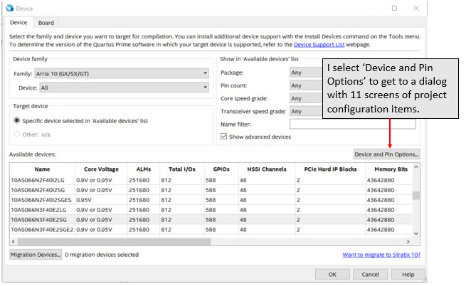
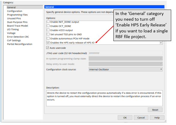
The Quartus setting that determines if your compile is flat or partial reconfiguration is quite obscure. If you look at the dialog from the ‘Device’ item in the ‘Assignments’ menu (I am using Quartus v17.0.2 so this could be different if the Quartus version is different) there is a button titled ‘Device and Pin Options’. When you press this you get a new dialog with 11 categories of project settings. The one setting that changes a project between Partial Reconfiguration and Flat design is in the ‘General’ category and it is at the bottom of the scrolled list, and it is titled ‘Enables the HPS early release of HPS IO’. If this is checked the compile makes a requirement that you use a xxx.periph.rbf and a xxx.core.rbf file. It does not cause the periph and core files to be generated, it only makes them required to boot using uboot. If it is not checked Quartus only creates one .SOF file (which you will later convert to an .RBF file for loading onto your SD Card) and this is all you will need to boot. (If you need to know how to make the other two .rbf files needed for Partial Reconfiguration let me know and I’ll send the tcl commands to do that.)
image

image

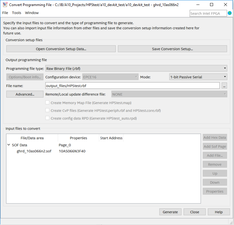
After compiling you convert your flat design .SOF file to an RBF (using the ‘Convert Programming Files’ item under the ‘File’ menu). You can name the RBF file any name you like but it has to have the RBF suffix. Start by chaning the ‘Programming File Type’ to RBF, then select the SOF Data Item down below and click on the ‘Add file’ button. Select your project’s .SOF file in the file dialog and wait for it to load. Now select the file browse button (’…’) next to the output ‘File Name’ above (this will ensure that it places your .RBF file in the output directory along with your other output files). Then click on the ‘Generate’ button at the bottom of the dialog.

The QSYS and Compile generated the handoff files in /hps_isw_handoff subdirectory which will be used to create the uboot loader file. These files are emif.xml and hps.xml. If your QSYS design does not include an emif component for the HPS processor then it will not create the emif.xml file. If you do not have the emif.xml file then the uboot generator will not work. So even if you do not plan to use any on-chip memory from your HPS you must include the emif component.

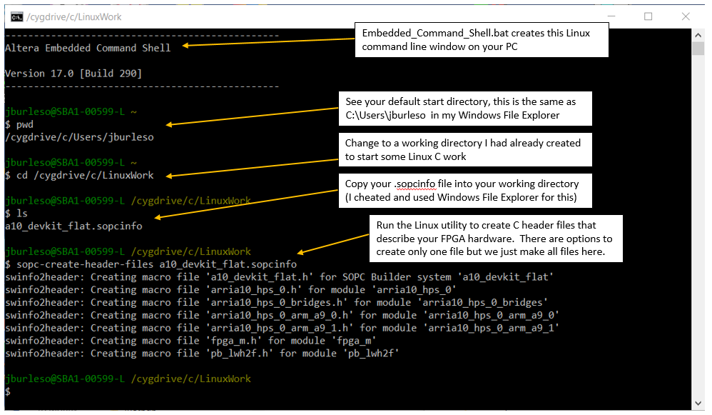
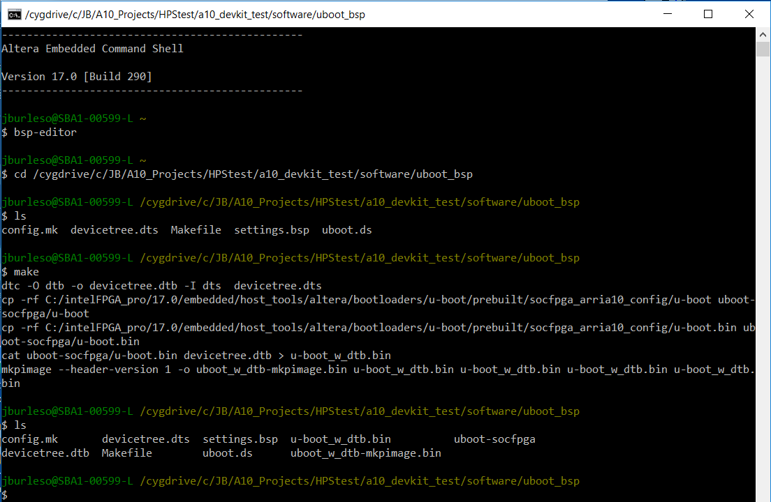
I run the bsp-editor tool from a SOCEDS shell window to create the source files to make a uboot boot file I can use to start my application from the SDCard when the board powers up. To do this in Windows navigate to your Quartus install directory and find the embedded directory (on my machine it is C:\intelFPGA_pro\17.0\embedded ) and execute the program Embedded_Command_Shell.bat. This creates a Linux command window. From the Linux command window run the BSP Editor by entering bsp-editor at the command prompt.

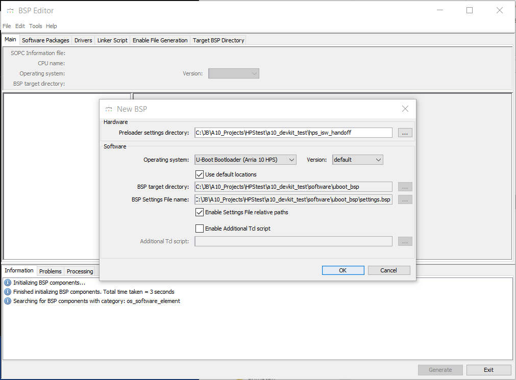
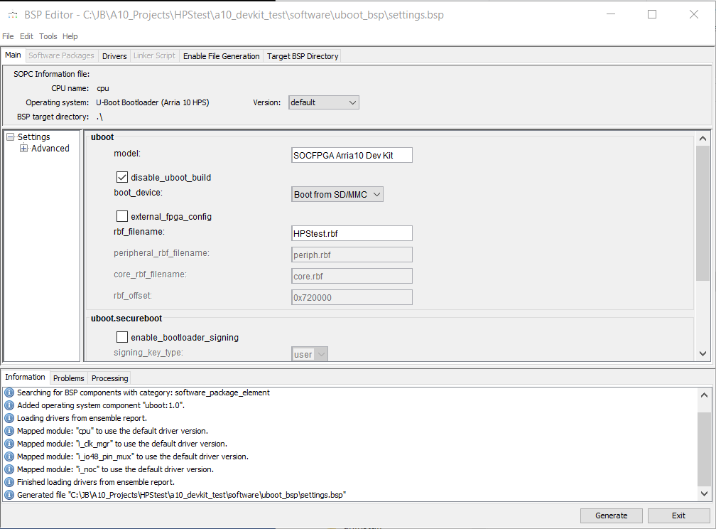
When the window comes up select ‘File’, then ‘New HPS BSP’ and select the ~/hps_isw_handoff directory for your project in the Preloader Settings Directory item. Also use the default locations os the outut files are written to the ~/software directory. When you click OK it will generate some files and present some new entry items. In this window ensure that ‘SOCFPGA Arria 10 Dev Kit’ is selected, and ensure the ‘disable uboot_build_boot_device’ box is checked, then enter your project’s RBF file name. Now click on ‘Generate’ and it will create some C project files. You can now exit the bsp-editor.

In the SOCEDS Linux window change directory to the uboot source directory specified in the bsp-editor (normally in the /software/uboot_bsp directory ) where you will find some C code files. You can build the project by entering ‘make’ at the Linux prompt.

This will generate two new files uboot_w_dtb_mkpimage.bin and uboot_w_dtb.bin
Copy the uboot_w_dtb-mkpimage.bin to your SD Card. This will be used in partition 3, but if you do this from Windows you will most likely only see partition 1 in the File Manager so you will already be placing files in that place. If you copy the files over to your HPS Linux system (so they could end up in whatever your current working directory is) you can copy the .rbf into partition 1 with the commands below. (Don’t enter the comment portions of the lines below --after the ‘–’ part.)

fdisk -l – this is to discover the SDcard partitions, but we already know where they should be
mkdir /media/sdcard – I usually create a directory for mounting the SD Card in
mount -v /dev/mmcblk0p1 /media/sdcard
cp .rbf /media/sdcard
umount /media/sdcard – dont forget to un-mount the sd card after you are done writing to it

You need a different command to install the uboot binary file into partition 3 (this has to be done in HPS Linux – though I am sure there is a way to do it from Windows but I do not know how) so use the command below to install the uboot into partition 3.

dd if=uboot_w_dtb-mkpimage.bin of=/dev/mmcblk0p3 bs=64k seek=0

Assuming all goes well you are ready to shut down and restart Linux.

shutdown -h now

I generally have about a dozen xxx.rbf files in my partition 1 at any time. Since the uboot is directed to a particular .RBF filename I just rename or copy the RBF files so the one I want to use is in place with the correct name to be booted for the next time the SD Card boots up. This works OK as long as you aren’t adding new devices that you dont have in your current device tree. I need to get around to rebuilding my device tree soon anyway – but that will come later.

It is a very good idea to back up your SD Cards, and a very very good idea when experimenting with new procedures for adding things and removing things from them. That being said I hope you make it safely through the process above and can get started on some straight-forward development using flat design projects.

1 Like

thank you ,
dose the SDcard contain a linux already ? or it should empty when following these instruction?

Yes, the SD Card should already have Linux installed. The instructions above are intended for modifying an existing SD Card. If a rebuild of the Angstrom Linux or the device tree is needed that is separate from the instruction steps listed.

1 Like

@Jambie
Please can you share your quartus project file. The link at file dropper is not working. Please I really need your file to see how to do communication between HPS and FIFO.

@Jambie
I follow this tutorial and tried to figure out how to send data back and forth on DE1-SoC

In the .c file, I found that the code that sends data to the FIFO is

	// send array to FIFO and read block
	for (i=0; i<N; i++){
		// wait for a slot
		// do the FIFO write
		FIFO_WRITE_BLOCK(data[i]);

I wonder where is FIFO_WRITE_BLOCK ?
Because in the system verilog file I can’t see how it take the data from the FIFO_WRITE_BLOCK

The HPS processors and the FPGA communicate via memory regions that are set aside for special purposes. In this case the purpose is to operate FIFOs. In this program example there are two FIFOs, one to communicate from the HPS to the FPGA, and one to communicate from the FPGA to the HPS. The two FIFOs really operate the same with just the intended direction of data and control signals being opposite.

Each FIFO has two memory regions that are shared between the HPS and the FPGA. One of the regions is for the data being exchanged between the two devices and one is for control and status (CSR) information. The control and status area uses the addresses as registers that are used to read that status of the FIFO. In our case here the first CSR address reports how many items are stored in the FIFO, and the second register has status bits with bit 0 being the ‘full’ bit and bit 1 being the “empty” bit. We use these to direct the FIFO operation. The CSR registers are all 32bits even when we don’t use all of the bits.

The data passed into (or out of) the FIFO is just written (or read) using C pointer indirection. This is implemented here using C macro definitions in the top portion of the example C code files (example shown below). The C macro definition can be seen in the definitions in the portion of the C file below for the FIFO_WRITE_BLOCK macro.

#define FIFO_WRITE_BLOCK(a) {while (WRITE_FIFO_FULL){WAIT};FIFO_WRITE=a;}

How it works is when the text FIFO_WRITE_BLOCK(data[i]); is used in the C code it is substituted with the definition of the macro that is found in the C file (or sometimes in a header file).
So the FIFO_WRITE_BLOCK(data[i]);
is replaced with
{while (WRITE_FIFO_FULL){WAIT};FIFO_WRITE=data[i];}
But since this macro definition contains other macro’s (also defined at the upper section of the C code) like WRITE_FIFO_FULL, and WAIT, and FIFO_WRITE then these will also be replaced by their defined replacements.
So the {while (WRITE_FIFO_FULL){WAIT};FIFO_WRITE=data[i];}
is replaced by (comments added by me to show what the lines are doing)
NOTE - ROCKETBOARDS EDITOR REMOVES SOME * CHARS SO THE SEGMENT BELOW
IS MISSING SOME POINTER REFERENCES - TRYING TO FIX THIS!!!
{
while ((((FIFO_write_status_ptr+1))& 1 )) // checks the FULL bit in CSR register
{}; // if the FIFO is full we do nothing here
(
(FIFO_write_ptr)) = data[i]; // once the FIFO is not FULL we assign the data to be
// written into the FIFO
}
which is completely C code statements.
The pointers used here FIFO_write_status_ptr and FIFO_write_ptr were set in the section of code (copied below) where we mapped (using the mmap() function) to the address space reserved for the FIFO hardware. This address space is shared by the HPS processors and the FPGA, so as the HPS or FPGA writes to addresses in the space the other side (HPS or FPGA) can read the values written.

//============================================

// get virtual addr that maps to physical
// for light weight bus
// FIFO status registers
h2p_lw_virtual_base = mmap( NULL, HW_REGS_SPAN, ( PROT_READ | PROT_WRITE ), MAP_SHARED, fd, HW_REGS_BASE );
if( h2p_lw_virtual_base == MAP_FAILED ) {
if(term_out == 1)
printf( “ERROR: mmap1() failed…\n” );
else
printf(“0\n0\n0\n0\n”);
close( fd );
return(1);
}
// the two status registers
FIFO_write_status_ptr = (unsigned int *)(h2p_lw_virtual_base);
// From Qsys, second FIFO is 0x20
FIFO_read_status_ptr = (unsigned int *)(h2p_lw_virtual_base + 0x20); //0x20

// ===========================================
// FIFO write addr
h2p_virtual_base = mmap( NULL, FIFO_SPAN, ( PROT_READ | PROT_WRITE ), MAP_SHARED, fd, FIFO_BASE);

if( h2p_virtual_base == MAP_FAILED ) {
	if(term_out == 1)
		printf( "ERROR: mmap3() failed...\n" );
	else
		printf("0\n0\n0\n0\n");
	close( fd );
	return(1);
}

// Get the address that maps to the FIFO read/write ports
FIFO_write_ptr =(unsigned int *)(h2p_virtual_base);
FIFO_read_ptr = (unsigned int *)(h2p_virtual_base + 0x10); //0x10

There are more macro definitions made in the C example files than we actually use in the examples but a good exercise is to translate some into the code they produce when you run into one you are not familiar with.