Hello, I am currently trying to get FPGA-SDRAM bridge working.
I have my own QSYS component containing Avalon MM Master which looks like this:
module sdram_if # (
  parameter ADDR_SIZE = 32,
  parameter DATA_SIZE = 256 )
( clk, reset,
avm_m0_read, avm_m0_write, avm_m0_writedata, avm_m0_address, avm_m0_readdata, avm_m0_readdatavalid, avm_m0_response, avm_m0_writeresponsevalid, avm_m0_byteenable, avm_m0_waitrequest, avm_m0_burstcount,
address, byteenable, read, data_out, write, data_in, busy );

// clk and reset are always required.
input logic clk;
input logic reset;
// Avalon Master ports
output logic avm_m0_read;
output logic avm_m0_write;
output logic [DATA_SIZE-1:0] avm_m0_writedata;
output logic [ADDR_SIZE-1:0] avm_m0_address;
input logic [DATA_SIZE-1:0] avm_m0_readdata;
input logic avm_m0_readdatavalid;
input logic [1:0] avm_m0_response;
input logic avm_m0_writeresponsevalid;
output logic [(DATA_SIZE/8)-1:0]avm_m0_byteenable;
input logic avm_m0_waitrequest;
output logic [10:0] avm_m0_burstcount;
// External conduit
input logic [ADDR_SIZE-1:0] address;
input logic [(DATA_SIZE/8)-1:0] byteenable;
input logic read;
output logic [DATA_SIZE-1:0] data_out;
input logic write;
input logic [DATA_SIZE-1:0] data_in;
output logic busy;

localparam INIT = 3'd0;
localparam READ_START = 3'd1;
localparam READ_END = 3'd2;
localparam WRITE_START = 3'd3;
localparam WRITE_END = 3'd4;

logic [2:0] cur_state;
logic [2:0] next_state;

logic [ADDR_SIZE-1:0] addr;
logic [DATA_SIZE-1:0] data;
logic [(DATA_SIZE/8)-1:0] enable;

// Handling change of the current state to the next requested state
always_ff @(posedge clk) begin
  if (reset) begin
    cur_state <= INIT;
  end else begin
    cur_state <= next_state;

    if (read) begin
      addr <= address;
      enable <= byteenable;
    end else begin
      if (write) begin
        addr <= address;
        enable <= byteenable;
        data <= data_in;
      end
    end
  end
end

// Handling FSM transitions
always_comb begin
  next_state = cur_state;
  busy <= '0;
  case(cur_state)
    INIT: begin
      if (read) begin
        next_state = READ_START;
      end else begin
        if (write) begin
          next_state = WRITE_START;
        end
      end
    end

    READ_START: begin
      busy <= '1;
      if (avm_m0_waitrequest) next_state = READ_START; // Wait here.
      else next_state = READ_END;
    end

    READ_END: begin
      busy <= '1;
      if (!avm_m0_readdatavalid) next_state = READ_END; // Wait here.
      else next_state = INIT;
    end

    WRITE_START: begin
      busy <= '1;
      if (avm_m0_waitrequest) next_state = WRITE_START; // Wait here.
      else next_state = WRITE_END;
    end

    WRITE_END: begin
      busy <= '1;
      next_state = INIT;
    end

    default: begin
      next_state = INIT;
    end
  endcase
end

// Handling read and write start of each transaction
always_comb begin
  avm_m0_address = '0;
  avm_m0_read = '0;
  avm_m0_write = '0;
  avm_m0_byteenable = '0;
  avm_m0_burstcount = '0;
  avm_m0_writedata = '0;

  case(cur_state)
    READ_START: begin
      avm_m0_address <= addr;
      avm_m0_read = '1;
      avm_m0_byteenable <= enable;
      avm_m0_burstcount = '1;
    end

    WRITE_START: begin
      avm_m0_address <= addr;
      avm_m0_write = '1;
      avm_m0_writedata <= data;
      avm_m0_byteenable <= enable;
      avm_m0_burstcount = '1;
    end

    default: begin
    end
  endcase
end

// Handling read and write end of each transaction
always_ff @(posedge clk) begin
  if (reset) begin
    data_out <= '0;
  end else begin
    case (cur_state)
      READ_END: begin
        if (avm_m0_readdatavalid) begin
          data_out <= avm_m0_readdata;
        end
      end

      default: begin
      end
    endcase
  end
end

endmodule
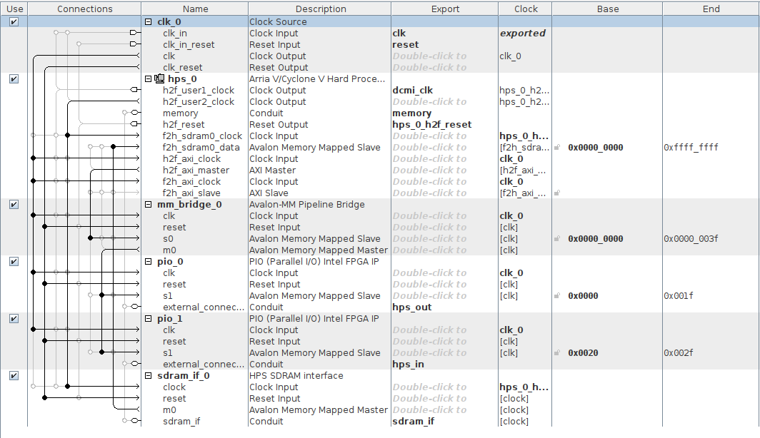
It’s wired in the Platform Designer like this:
I also have VHDL entity for testing, the process accessing the SDRAM looks like this:
count : PROCESS (nrst, clock) IS
  VARIABLE counter : INTEGER := 0;
  VARIABLE ticks : INTEGER := 0;
  VARIABLE write_en : STD_LOGIC := '0';

  CONSTANT START_ADDR : STD_LOGIC_VECTOR(31 DOWNTO 0) := STD_LOGIC_VECTOR(to_unsigned(16#2000_0000#, 32));
  CONSTANT BYTE_ENABLE : STD_LOGIC_VECTOR(31 DOWNTO 0) := (OTHERS => '1');
BEGIN
  IF nrst = '0' OR h2f_nrst = '0' THEN
    sdram_data_write <= (OTHERS => '0');
    sdram_address <= (OTHERS => '0');
    sdram_byteenable <= (OTHERS => '0');
    sdram_read <= '0';
    sdram_write <= '0';

    i_led <= (OTHERS => '0');
    counter := 0;
    ticks := 0;
    write_en := '0';
  ELSE
    IF rising_edge(clock) THEN
      sdram_read <= '0';
      sdram_write <= '0';
      sdram_data_write <= (OTHERS => '0');
      sdram_address <= (OTHERS => '0');
      sdram_byteenable <= (OTHERS => '0');

      IF counter = 50_000_000 THEN -- every 1 sec
        counter := 0;
        IF write_en = '0' AND ticks = 30 THEN -- delay writing by 30 sec
          write_en := '1';
          i_led(7) <= '1';
          ticks := 0;
        END IF;
        IF write_en = '1' THEN
          sdram_address <= START_ADDR;
          sdram_data_write(31 DOWNTO 0) <= STD_LOGIC_VECTOR(to_unsigned(ticks, 32));
          sdram_byteenable <= BYTE_ENABLE;
          sdram_write <= '1';
        END IF;
        ticks := ticks + 1;
        i_led(0) <= NOT i_led(0);
      ELSE
        counter := counter + 1;
      END IF;
    END IF;
  END IF;
END PROCESS;
I am checking the SDRAM content from HPS using memtool. The problem is the address keeps incrementing by 16B (256 bits, data width) even when it should remain fixed to 0x2000_0000. Sometimes there is a delay before first write transaction occurs for some reason, also sometimes write transactions stop happening or the address goes back to the start.
Example memory content looks like this (I also highlighted an adress when I released the reset button - the counter did reset but the address did not):
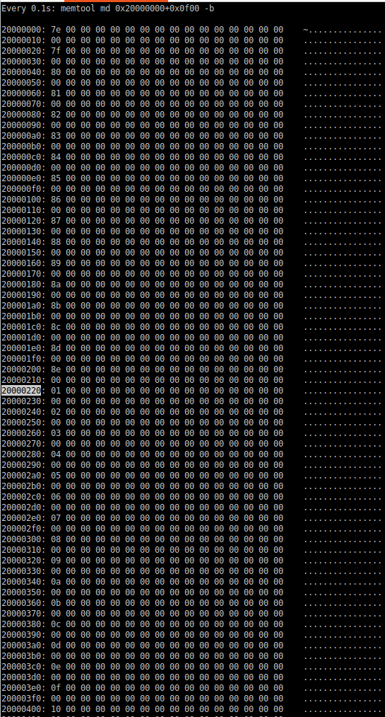
What am I doing wrong? Why the address keeps incrementing and how to fix it?
Thank you for any suggestions!