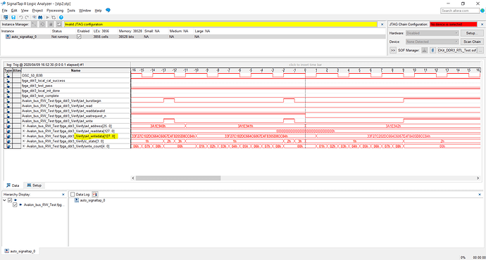
Hello all, I am trying to understand the DDR3 SDRAM design example from the TERASIC cyclone V board. It has an example design that comes with the Native PHY IP core of DDR3 SDRAM. Can anyone help me understand the code? I have following questions
- What are y1, y2 and z and why the wire Y is written in a format which depends upon Y1 and Y2 and Z? Can’t I write a data directory without doing all this stuff?
assign y0 = cal_data + {44’b0, avl_address};
assign y1 = {y0[31:0], y0[63:32]} ^ cal_data;
assign y2 = y1 + cal_data;
assign z = y1[7:0] + y2[7:0];
assign y = {y2[61:5],z,y2}; - SDRAM has active low avl_waitrequest_n so why in state 2 avl_write is 0 when I have high avl_waitrequest_n?
- In state 5, why avl_read is 0 when I am reading data from avalone as data_reg <= avl_readdata;
I shall highly appreciate any help as this is my first post in this forum.
Here is the entire code.
module Avalon_bus_RW_Test (

		iCLK,
		iRST_n,
		iBUTTON,

		local_init_done,
		avl_waitrequest_n,
		avl_address,
		avl_readdatavalid,
		avl_readdata,
		avl_writedata,
		avl_read,
		avl_write,
		avl_burstbegin,

		drv_status_pass,
		drv_status_fail,
		drv_status_test_complete,

		c_state


);

parameter      ADDR_W             =     26;
parameter      DATA_W             =     128;

input          iCLK;
input          iRST_n;
input          iBUTTON;
input				local_init_done;
input          avl_waitrequest_n;                 //             avl.waitrequest_n
output [ADDR_W-1:0]  avl_address;                       //                .address
input          avl_readdatavalid;                 //                .readdatavalid
input  [DATA_W-1:0] avl_readdata;                      //                .readdata
output [DATA_W-1:0] avl_writedata;                     //                .writedata
output         avl_read;                          //                .read
output         avl_write;                         //                .write

output		drv_status_pass;
output		drv_status_fail;
output		drv_status_test_complete;

output			avl_burstbegin;
output	[3:0]c_state;

//=======================================================
//  Signal declarations
//=======================================================
reg  [63:0]          clk_cnt, cal_data;
reg  [1:0]           pre_button;
reg                  trigger;
reg  [DATA_W-1:0]    data_reg;
wire [63:0]          y0, y1, y2;
wire [7:0]           z;
wire [DATA_W-1:0]    y;
reg  [3:0]           c_state;
reg	                avl_write, avl_read;
reg	 [ADDR_W-1:0]   avl_address;
reg	 [DATA_W-1:0]   avl_writedata;
reg  [4:0]            write_count;
wire                  max_avl_address;
wire                  same;


//=======================================================
//  Structural coding
//=======================================================
assign avl_burstbegin = avl_write || avl_read;

assign y0 = cal_data + {44'b0, avl_address};
assign y1 = {y0[31:0], y0[63:32]} ^ cal_data;
assign y2 = y1 + cal_data;
assign z = y1[7:0] + y2[7:0];
assign y = {y2[61:5],z,y2}; //

assign max_avl_address = &avl_address;
assign same = data_reg == avl_writedata;

always@(posedge iCLK)
  if (!iRST_n)
  	 clk_cnt <= 64'b0;
  else
  	 clk_cnt <= clk_cnt + 64'b1;


always@(posedge iCLK)
begin
	if (!iRST_n)
	begin
		pre_button <= 2'b11;
		trigger <= 1'b0;
		write_count <= 5'b0;
		c_state <= 4'b0;
		avl_write <= 1'b0;
		avl_read <= 1'b0;
	end
	else
	begin
		pre_button <= {pre_button[0], iBUTTON};
		trigger <= !pre_button[0] && pre_button[1];

	  case (c_state)
	  	0 : begin //idle
	  		avl_address <= {ADDR_W{1'b0}};
	  		if (local_init_done && trigger)
	  		begin
	  			cal_data <= clk_cnt;
	  			c_state <= 1;
	  		end
	  	end
	  	1 : begin //write
	  		avl_writedata <= y;
	  		if (write_count[3])
	  		begin
	  			write_count <= 5'b0;
	  		  avl_write <= 1'b1;
	  		  c_state <= 2;
	  		end
	  	  else
	  	  	write_count <= write_count + 1'b1;
	  	end
	  	2 : begin
	  		if (avl_waitrequest_n)
	  		begin
	  			avl_write <= 1'b0;
	  			c_state <= 3;
	  		end
	  	end
	  	3 : begin
	  	  if (max_avl_address)
	  		begin
	  			avl_address <=  {ADDR_W{1'b0}};
	  			c_state <= 10;
	  		end
	  		else
	  		begin
	  			avl_address <= avl_address + 1'b1;
	  			c_state <= 1;
	  		end
      end
		10 : c_state <= 11;
		11 : c_state <= 4;
	  	4 : begin //read
	  		avl_writedata <= y;
	  		avl_read <= 1;

	  		if (!write_count[3])
	  			write_count <= write_count + 1'b1;

	  		if (avl_waitrequest_n)
	  			c_state <= 5;
	  	end
	  	5 : begin //latch read data
	  		avl_read <= 0;

	  		if (!write_count[3])
	  			write_count <= write_count + 5'b1;

	  		if (avl_readdatavalid)
	  		begin
	  			data_reg <= avl_readdata;
	  			c_state <= 6;
        end
	  	end
	  	6 : begin
	  		if (write_count[3])
	  		begin
	  			write_count <= 5'b0;
	  			if (same)
	  				c_state <= 7;
	  			else
	  				c_state <= 8;
        end
        else
        	write_count <= write_count + 1'b1;
	  	end
	  	7 : begin
	  	  if (max_avl_address)
	  		begin
	  			avl_address <=  {ADDR_W{1'b0}};
	  			c_state <= 9;
	  		end
	  		else
	  		begin
	  			avl_address <= avl_address + 1'b1;
	  			c_state <= 4;
	  		end
	  	end
		8 : c_state <= 8;
		9 : c_state <= 9;
	    default : c_state <= 0;
	  endcase
  end
end

// test result
assign drv_status_pass = (c_state == 9) ? 1 : 0;
assign drv_status_fail = (c_state == 8) ? 1 : 0;
assign drv_status_test_complete = drv_status_pass || drv_status_fail;

endmodule