I’ve spent some time trying to decipher Altera’s FPGA-to-HPS design. I’ve looked at Platform Designer, their IP verilog files, as well as read online documentation regarding the individual modules (images are below). What I do not understand is how/where the FPGA fabric has access to read data from the DDR memory (i.e. need an explanation of the Qsys DMA /Memory/FPGA connection in the image below) ? Looking at the generated IP verilog files, I can see that the DMA is connected to the L3 interconnect but at no point are any signals exported from the DMA_system module or the arria_10_hps module in Platform Designer to give the FPGA user access to read data. How does the FPGA send the appropriate signals to receive data from the DDR ?
I am hoping my understanding of the system is correct. We could potentially cross-check that my comments are valid.
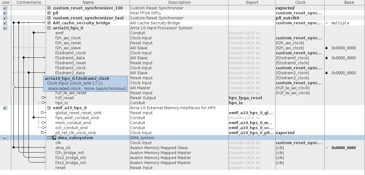
In the system you posted the screen-shot of, there are three access points to the HPS’ DDR-RAM:
The FPGA-to-HPS bridge (through the L3 interconnect).
The FPGA-to-SDRAM bridge 0.
The FPGA-to-SDRAM bridge 2.
The DMA sub-system is connected as a master to all of those ports. Also note that this DMA sub-system is not part of the HPS, but rather it will be implemented in the FPGA.
If you wanted to re-use this design, I guess you will need to disconnect the DMA from one of the bridges in order to allow your logic to use that port. Otherwise, you can also connect an arbiter to provide access to more masters.
Does this make sense or am I repeating something you already knew?
That does make sense. I was moving towards either exporting the ‘f2sdram0_data’ and ‘f2sdram0_clock’ signals or exporting the ‘Avalon memory mapped masters’ of the DMA (unsure as to which one would give me direct access to memory). From my understanding the DMA is implemented in hardware and so exporting its signals would make sense. However, the signal ports themselves are found on the ‘arria10_hps’ in the Qsys. My follow up question would be then what is the DMA exactly being used for? It seems that the DMA has an input from the ‘h2f_lw_awi_master’ (to perhaps control the reading from software?).
I think I have taken a look at this example design in the past, but I am not sure.
If I remember correctly, this design only show-cases how to use the DMA.
Remember that at the end of the day, a DMA engine just allows the processor to move data from one location to another.
What this means is that you need two things for the DMA:
A control port for the CPU to configure and trigger the DMA transactions, eg: I want to move X number of bytes from address A to address B. For this you have the “h2f_lw_axi_master”. “lw” stands for light-weight, this is a simplified AXI port used precisely for this purpose, control and monitoring of HW peripherals on the FPGA.
Connections from the DMA master ports (it can actually be only one), to the memory bus of the CPU.
In conclusion:
It is not completely bizarre to have this configuration where all the master ports of the DMA are connected to the fabric, if your HPS doesn’t need to communicate with any other peripherals in the FPGA.
If you want to have access from the FPGA to the HPS’s DDR you will need to “make a cut”, meaning, disconnect at least one of the DMA master ports. From there you have a couple of options…