Hi.
I am new with cyclone V FPGA (DE10 Nano), I dont understnad my VHDL code behaved different (Or stuck after some time), with different set of pin assignment.
like i tried to read a shared register (PIO- driven by external clock sourse) between FPGA and HPS, does work when i assign ext clock input pin to (PIN_AA24) but does not work when assigned to (Y15). //" and sometime stops working after some time"
In your case one of the pins is connected to an LED output pin and the other is connected to a gpio pin.
You can’t get any clock signal from an LED of course, and unless your gpio pin is connected to an external clock source it doesn’t make sense either.
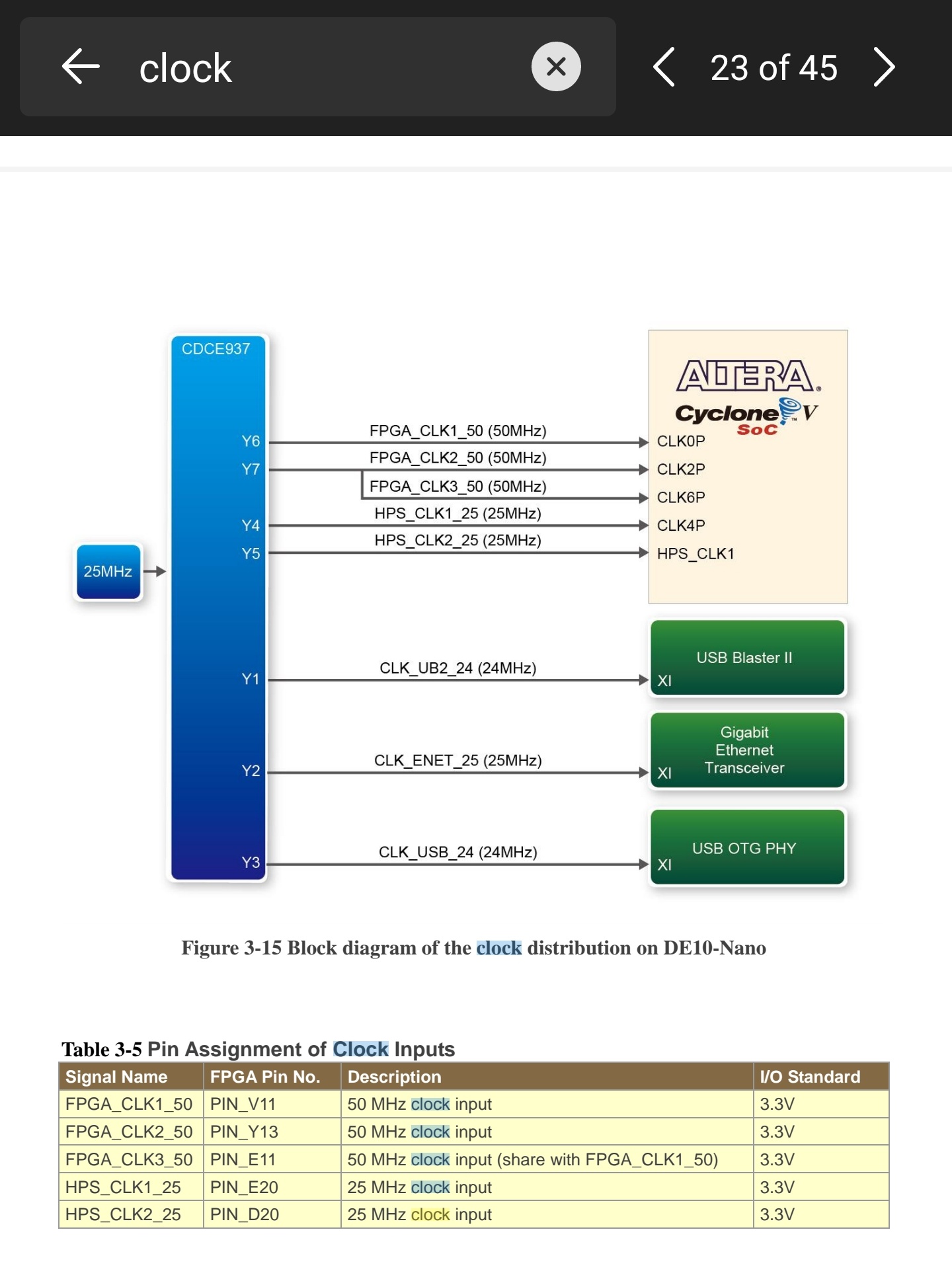
Those are the onboard clock sources on the de10 nano (from the de10 nano user manual):
The pin name in the pin assignment must match a port name from your top level entity so you can either:
Use the signal name from the user manual as the name of the port in your top level entity (the better option imo)
Ignore the signal name from the user manual and set the name in the pin assignment to the name of the port in your top level
You can (and should) export the pin assignments from any demo project that is already available for your board (I’d go for the GHRD demo project because it uses most/all of the onboard periphery).
Then import it to any project that uses that same board.
If you already use the signal names from the user manual as your top level’s ports names you don’t need to change anything.
After being struck for very long… i understand pin assignment must be done carefully…
De10 nano board cyclone V, my project consists of 4 niosii procs and HPS.
I experienced that. If I choose one pin from gpio bank… for proving input… it won’t work (works for some time then stops.) but if I just change the input pin from pin planner … it works like charm… !