I need to create a communication between Arm and FPGA of Arria 10 SoC devkit , i need to send data and receive data, i understand the idea on how to exchange data between them , what i don’t understand is the Qsys logic,
i sow a lot of examples but i can’t understand the logic behind them; how are the component in the Qsys are related to the VHDL design…
can anyone help me please ?
Thank you
Here I have a set of complete examples moving data from HPS and FPGA in Cyclone V SoC family.
You have 2 options:
-
Use the HPS as a master. you have to create a Qsys component with avalon slave interface. there are tutorials on doing that. You can connect this slave to HPS-FPGA or Lightweight HPS-FPGA bridges. To move data you can use processor or HPS DMA as explained in my examples.
-
Use FPGA as master: you have to create a component in the FPGA with master capabilities (avalon master or AXI master) and then write/read the HPS through the FPGA-HPS bridge or FPGA-SDRAMC bridge. This is more tricky because designing a master is more difficult than designing a slave. The master has to stop writing if the slave connected to it cannot accept more data.
They way VHDL and Qsys is related is through Qsys components. You first create a VHDL component. Then you go to Qsys and do create new component. In the new component menu you assign the ports you created in VHDL with standard signals of avalon or AXI bus, so later Qsys will interprete your signals as standard bus and connect them with a single click. For example what I do is to create a VHDL with reset_n, clk, wr, rd, address bus and data bus. Internally I create a bunch of registers and use these signals to access them. When creating a Qsys component I asign clk to avalon clock interface, reset_n to avalon reset interface, and the others to a avalon memory mapped interface.
I ve leart through the following tutorial: ftp://ftp.altera.com/up/pub/Altera_Material/15.1/Tutorials/making_qsys_components.pdf
Hope it helps
1 Like
thank you sir, this is helpful ,
Ok , now what i don’t understand is :
lets say i created a Qsys project and i added a HPS component one HPS2FPGA_FIFO and one FPGA2HPS_FIFO , an onchip_memory component … i connected the h2f bridge to the two fifos … and the Qsys project is finished ,now i want to build a VHDL design that reads from the first FIFO then process information and writs result to the second one,
what are the output signal ? should they be already exported on Qsys ?
I do not understand why you use fifo. do a drawing or explain better what data movement you wanna do. the easiest way i think is tah you use a double port onchip ram with 2 avalon buses. then one port is connected to hps through hps-fpga bridge and the other to other logic in your fpga that should have master capabilities to read and write the second port of the double port on chip
1 Like
Thank you sir for the reply ,
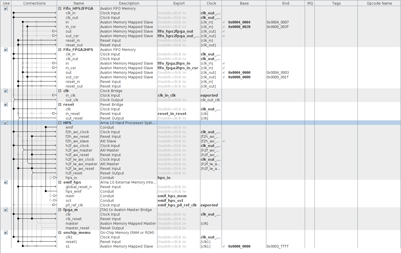
Ok ,i created a project from scratch with the help of this project 'https://rocketboards.org/foswiki/Projects/HPS2FPGA ’
what i want to do is to send 2 32bit integer to the FPGA to do the sum and then display the result on the linux terminal ,
this is the Qsys design